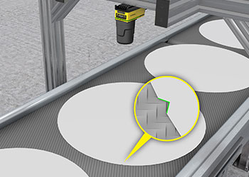
In the wafer manufacturing process, understanding the position and orientation of semiconductor wafers is critical. Each step is to understand the wafer orientation by monitoring the Notch slots on the wafer. Because wafer costs range from $5,000 to more than $100,000, any misalignment in the manufacturing process can cause serious and irreparable defects that can lead to wafer obsoletion.

The traditional way to find gaps is to use a through-beam array laser sensor, which requires bulky transmitters and receivers above and below the wafer. This takes up valuable mechanical space and wastes time because the wafer needs to be rotated all the way to the Notch slot. With the introduction of clear wafers (SiC) and other special wafer coatings, it has become more difficult for pass-beam sensors to accurately find Notch slots, increasing the chance of misalignment.
Cognex's In-Sight vision system accurately identifies wafer Notch and XY positions with an accuracy of up to 0.025 pixels. The Cognex PatMax algorithm accurately detects wafer Notch slots in any orientation and then transmits position and dimension data back to the assembly robot or PLC. In addition, the ultra-small shape design of the vision system can meet extremely narrow space constraints, eliminating the need to install laser optical sensors on and below the wafer.
If the manufacturer is unable to mount a lens over a longer working distance, Cognex also offers a patented low-altitude optical system to view the entire wafer.
Disclaimer: This article is from the Internet and is for the purpose of academic communication only. If there is any problem, please contact delete.
Phone:028-62705808
Fax:028-62705808
Mobile Phone:18215640190
Email:sales@cdxiwang.com
Address:2-8-6, Chen Electric Technology Innovation Park, 68 Shuangbai Road, High-tech West District, Chengdu