With the increasing popularity of electronic products, users have higher and higher requirements for their functions and quality. More and more manufacturers are using machine vision to help manufacture electronic components and devices to improve productivity and quality. In order to let more enterprises understand the solutions of the electronic product industry, the following Xinxiwang will introduce the application of Cognex products in semiconductor and printed circuit board assembly
Solutions for semiconductor applications
Throughout the manufacturing process of semiconductors on wafers, there are many inspection and measurement steps to ensure that the semiconductors are defect-free and assembled as designed. Cognex 2D and 3D machine vision inspection systems and deep learning technology enable the entire manufacturing process to optimize the entire manufacturing process by monitoring the diameter of the ingot at the time of formation, wafer notching detection, and inspection of die lead frames prior to wire bonding.
1. Wafer and die alignment
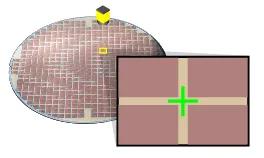
PatMax technology provides reliable, accurate, and fast wafer and die pattern positioning for wafer inspection, probing, mounting, dicing, and test equipment.
2. Wafer and IC package identification
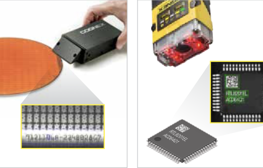
The In-Sight 1740 series barcode readers are capable of reading tricky wafer ID identifications. DataMan barcode readers can trace lead frames and IC packages through final assembly and device testing.
3. Semiconductor testing
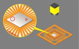
PatMax technology is able to locate and detect surface defects such as probe marks, cracks, or chips that affect die quality.
4. Wafer notch detection
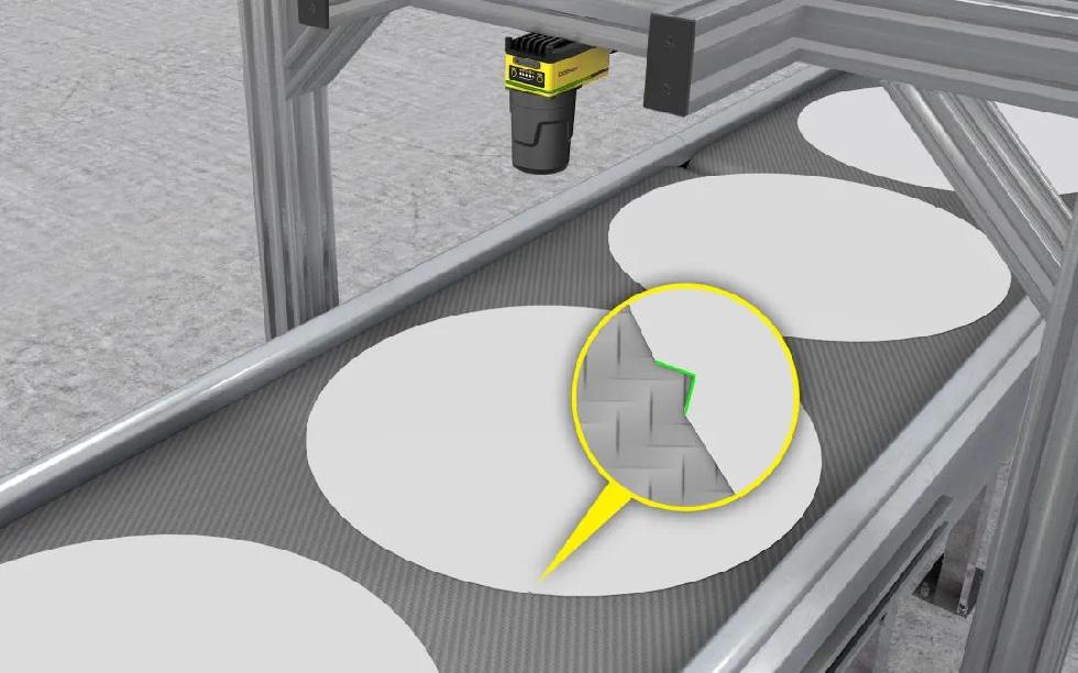
The In-Sight vision system and PatMax technology accurately identify wafer notches and XY positions from any orientation.
Solutions for printed circuit board assembly applications
The printed circuit board (PCB) assembly process involves complex alignment, bead bonding, and soldering steps, and requires ensuring that all small components are connected without defects and properly assembled onto the board. Cognex technology enables manufacturers to ensure that PCB components and assemblies are assembled and functioning properly, guaranteeing production quality.
1. Laser drilling and scribing alignment
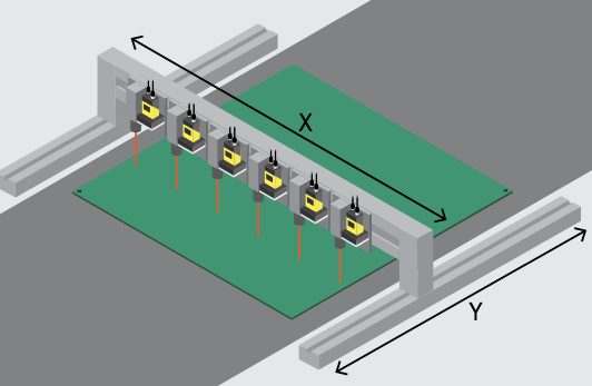
AlighSight sensors are able to quickly automate vision-motion control calibration to ensure accurate alignment between the drilled hole and the PCB board.
2. PCB assembly placement guide
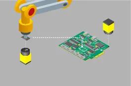
Machine vision solutions can guide robots to place components onto PCBs, including surface mount equipment.
3. PCB reference point alignment
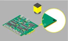
During screen printing, dispensing, mounting, and automated optical inspection, PatMax technology uses geometry information to locate fiducial markers.
4. Printed circuit board identification
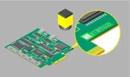
Advanced barcode reading technology is able to identify serial numbers on circuit board assemblies and read codes on PCBs for traceability.
5.PCB detection
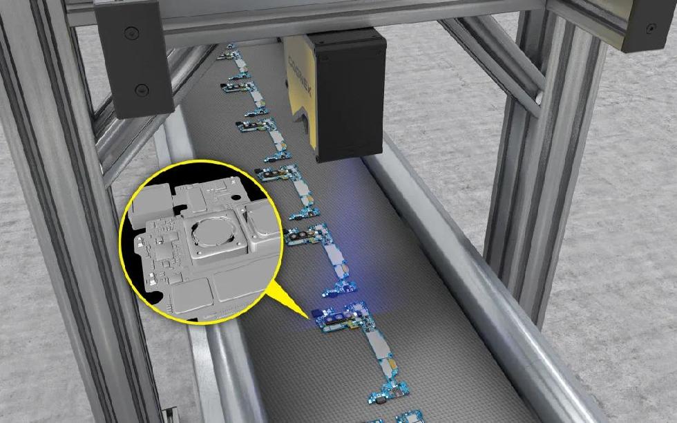
2D and 3D machine vision systems reliably inspect PCBs to ensure the correct number, size, and position of components.
6. PCB assembly verification
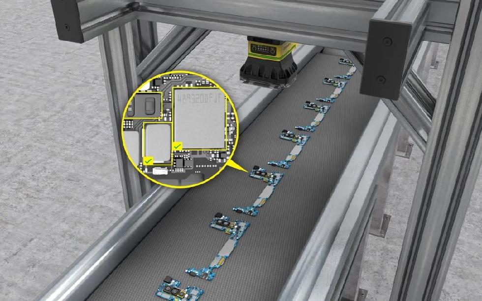
Cognex deep learning software can identify components based on distinguishing features and learn their correct position on the board.
7. OCR on PCB assembly components

Cognex Deep Learning Software's OCR tool is capable of reading a wide range of character text in challenging conditions.
8. Chip positioning and alignment measurement
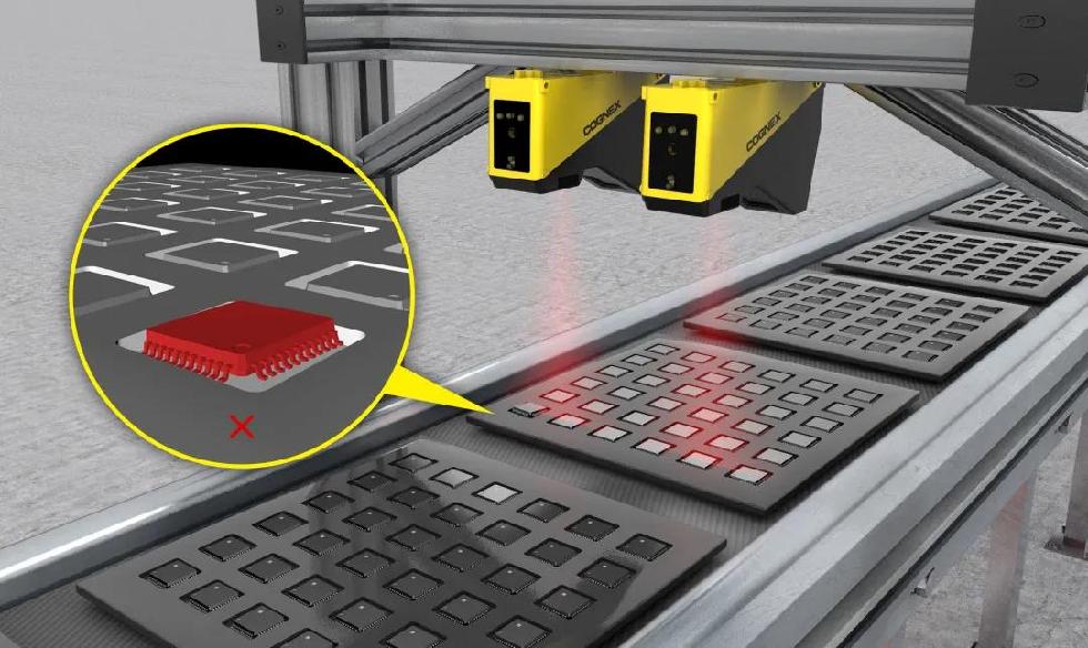
The 3D laser displacement sensor is able to accurately detect individual skewed chips on the outgoing pallet.
9. Multilayer ceramic capacitor detection
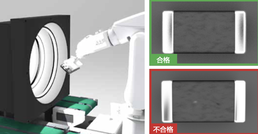
Multilayer Ceramic Capacitor (MLCC) visual inspection equipment makes full use of custom light sources and deep learning tools to identify defects in the capacitor body and terminals.
Disclaimer: Some of the content and pictures in this article are from the Internet, which is only for the purpose of academic communication. If there is anything wrong, please contact us to delete it.
For more information about Cognex products and solutions, please call 028-62705808
Phone:028-62705808
Fax:028-62705808
Mobile Phone:18215640190
Email:sales@cdxiwang.com
Address:2-8-6, Chen Electric Technology Innovation Park, 68 Shuangbai Road, High-tech West District, Chengdu